Designing and Simulating a CMOS inverter using Electric VLSI (second pass)
So far the design and simulation of the inverter has been completely tangled.
The focus of this tutorial is to “separate” design and simulation.
The strategy to achieve this goal consists of 3 steps:
create a schematic containing only the inverter circuit (no stimuli, no analyses)
<–> i.e. a schematic containing only the designassociate the schematic of the inverter's circuit to a symbol
create a schematic with symbol, stimuli and analyses
<–> i.e. a schematic for running the simulation (a.k.a. testbench)
1. start electric
2. open the library C5_CMOSLIB
File > Open Library
3. duplicate the cell C5_inverter_VTC(sch) as inv_20_10(sch)
use Cell –> Duplicate Cell
4. modify the schematic of the cell inv_20_10(sch) as follows:
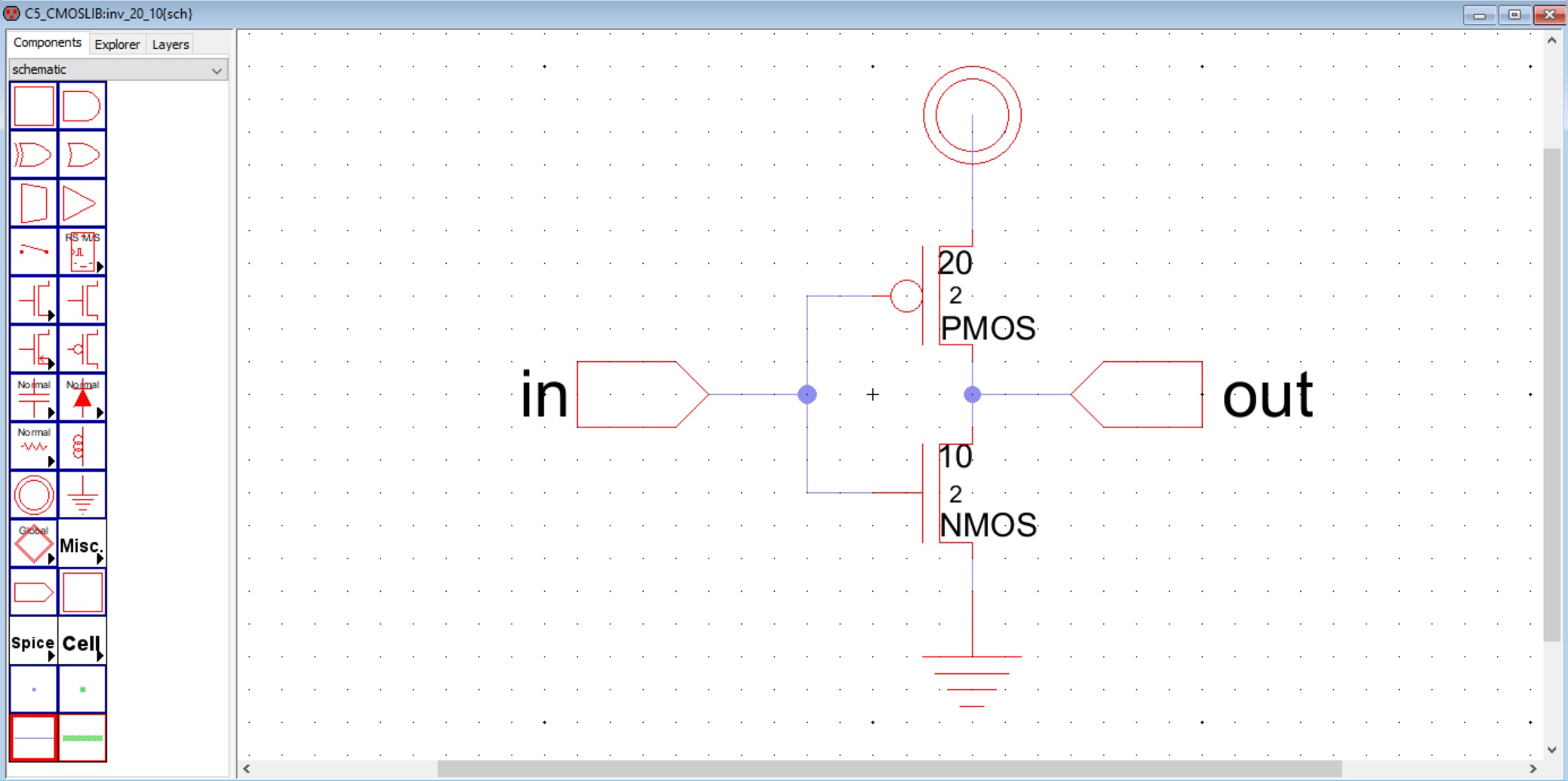 |
instantiate the input and output port from the palette of components
name the ports using Export > Create Export
 |
check the schematic's correctness (Tools > DRC > Check Hiererchically | F5)
5. generate a symbol for the schematic
use View > Make Icon View
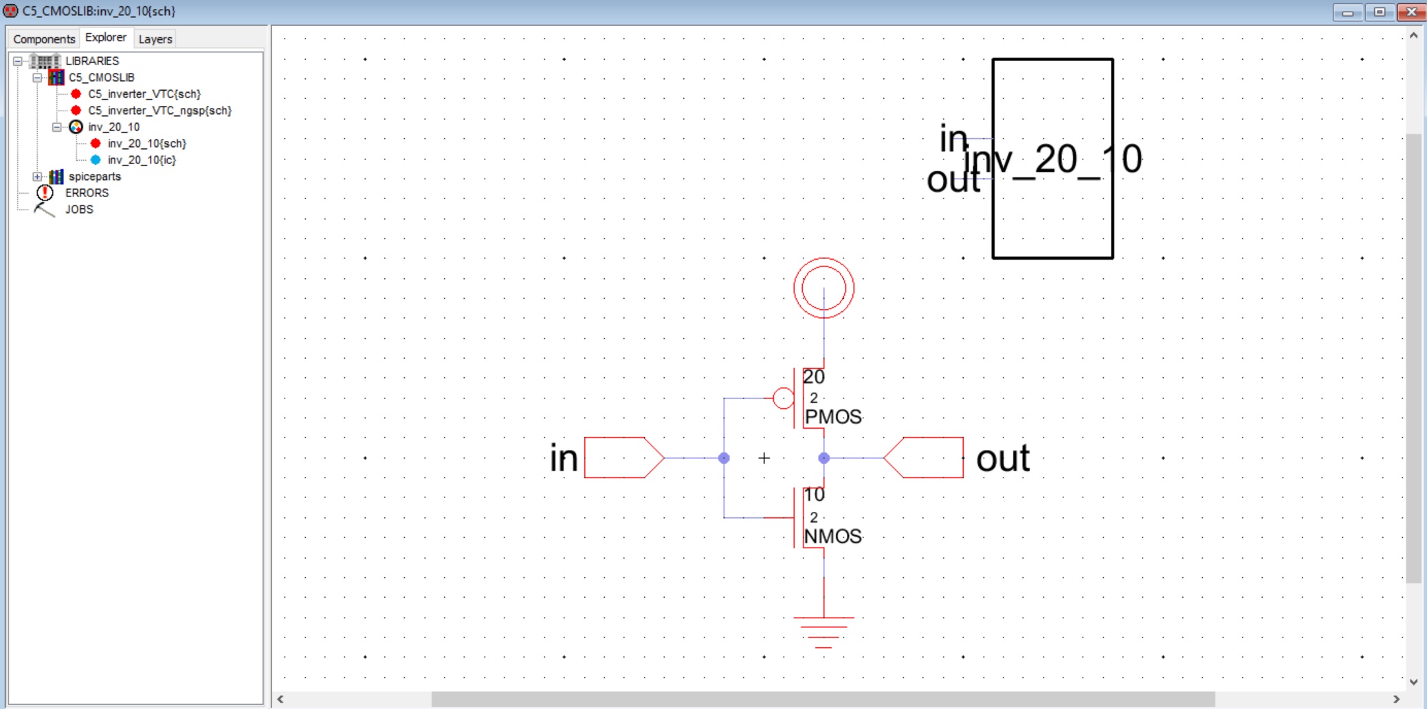 |
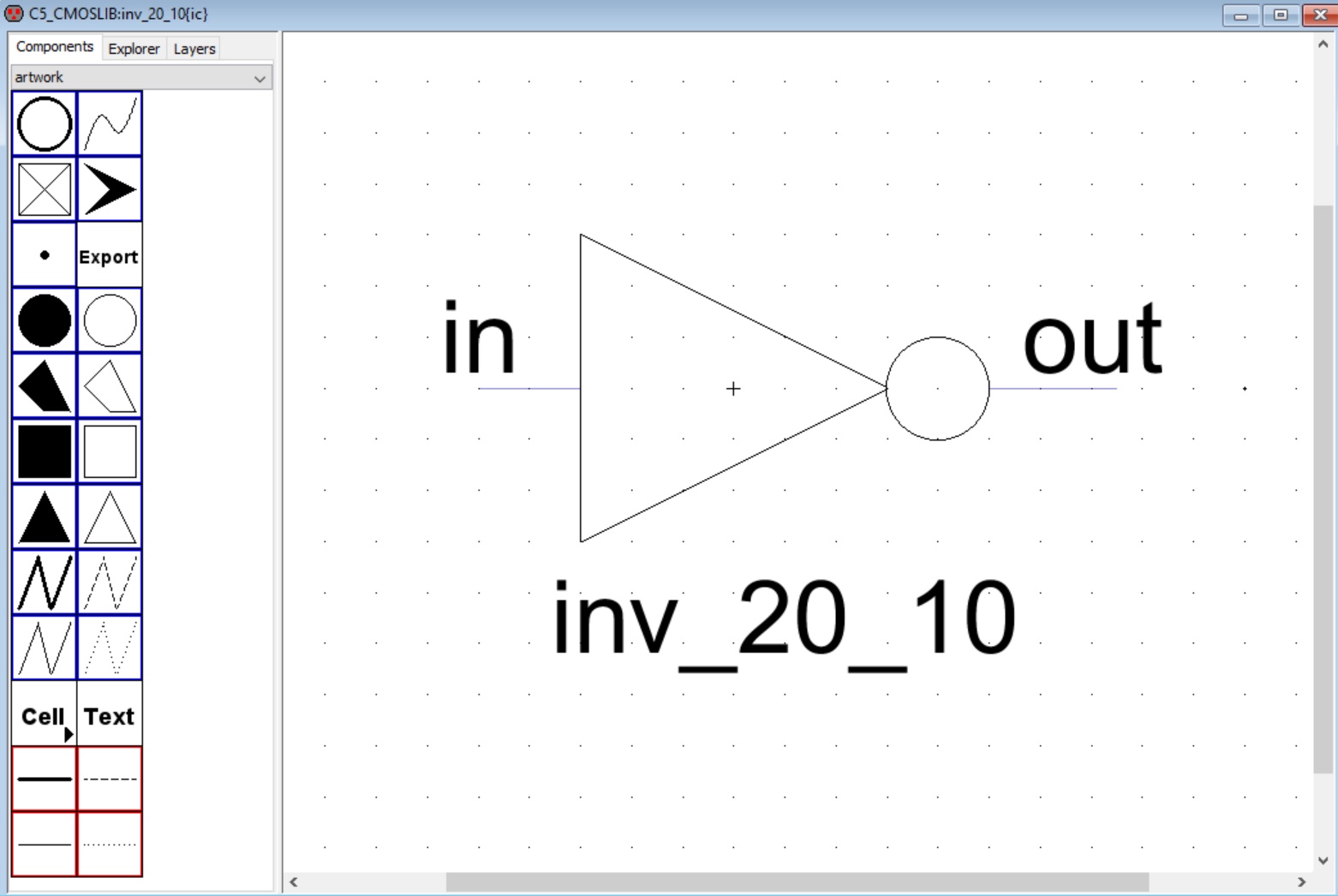
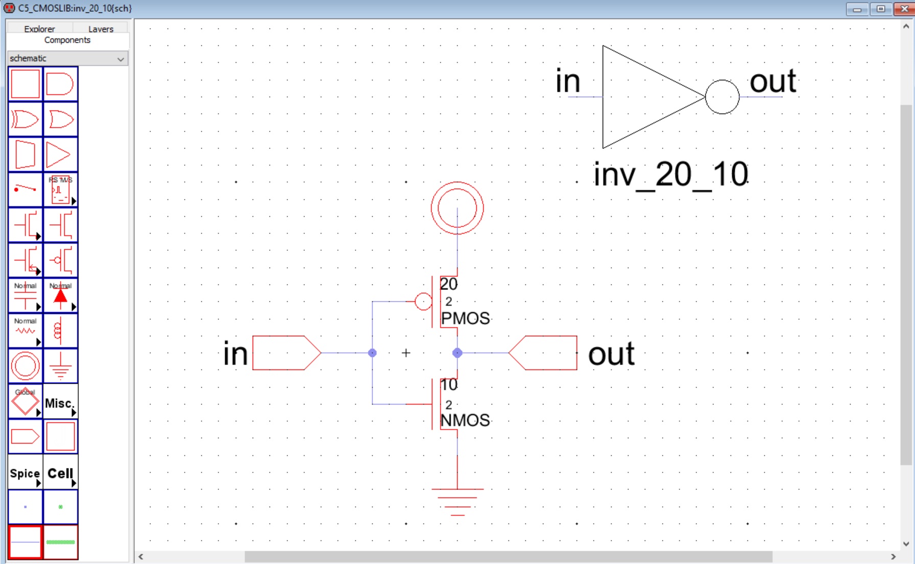
6. open the icon and edit its appearance
from within the schematic inv_20_10(sch) select the icon and click E
or go to the explorer panel and double click on inv_20_10(ic)edit the icon to look as follows:
 |
 |
6. a few more frequently used commands and their bindings
Cell > Down Hierarchy > Down Hierarchy | E
Cell > Up Hierarchy > Up Hierarchy | Ctrl + E
Edit > Size > Interactively | Ctrl + B
7. create a schematic with both the inverter's symbol and the simulation directives (stimuli & analyses)
Cell > New Cell
 |
modify the cell C5_inverter_TRAN(sch) as follows:
|
|
use the key binding F5 to check the correctness of the schematic (DRC = Design Rule Check)
8. simulate the design with ngspice
use the key binding Shift S
|
|
the spice netlist simulated is:
*** SPICE deck for cell C5_inverter_TRAN{sch} from library C5_CMOSLIB
*** Created on Tue Nov 09, 2021 19:47:42
*** Last revised on Tue Nov 09, 2021 20:02:28
*** Written on Tue Nov 09, 2021 21:15:43 by Electric VLSI Design System, version 9.07
*** Layout tech: mocmos, foundry MOSIS
*** UC SPICE *** , MIN_RESIST 4.0, MIN_CAPAC 0.1FF

*** SUBCIRCUIT C5_CMOSLIB__inv_20_10 FROM CELL inv_20_10{sch}
.SUBCKT C5_CMOSLIB__inv_20_10 in out
** GLOBAL gnd
** GLOBAL vdd
Mnmos@2 out in gnd gnd NMOS L=0.6U W=3U
Mpmos@0 vdd in out vdd PMOS L=0.6U W=6U
.ENDS C5_CMOSLIB__inv_20_10

.global gnd vdd

*** TOP LEVEL CELL: C5_inverter_TRAN{sch}
Xinv_20_1@0 in out C5_CMOSLIB__inv_20_10

* Spice Code nodes in cell cell 'C5_inverter_TRAN{sch}'
vdd vdd 0 DC 5
vin in 0 pulse(0 5 0 1n 1n 4n 10n)
.include ../../class/models/C5_models_bsim3.mod
.tran 100p 30n
.plot tran v(in) v(out)
.END
the simulation log file is:
Compatibility modes selected: hs a

Circuit: *** spice deck for cell c5_inverter_tran{sch} from library c5_cmoslib

Warning: Model issue on line 11 :
  .model nmos nmos ( level=49 version=3.1 tnom=27 tox=1.39e-8 xj=1.5e-7 nc ...
unrecognized parameter (xl) - ignored
unrecognized parameter (xw) - ignored
Warning: Model issue on line 13 :
  .model pmos pmos ( level=49 version=3.1 tnom=27 tox=1.39e-8 xj=1.5e-7 nc ...
unrecognized parameter (xl) - ignored
unrecognized parameter (xw) - ignored
ASCII raw file "C5_inverter_TRAN.raw"
Doing analysis at TEMP = 27.000000 and TNOM = 27.000000

Warning: Pd = 0 is less than W.
Warning: Ps = 0 is less than W.
Warning: Pd = 0 is less than W.
Warning: Ps = 0 is less than W.
Warning: vin: no DC value, transient time 0 value used
No. of Data Columns : 6

Initial Transient Solution
--------------------------

Node                                   Voltage
----                                   -------
out                                          5
in                                           0
vdd                                          5
vin#branch                                   0
vdd#branch                        -1.50033e-11

No. of Data Rows : 341
.plot line ignored since rawfile was produced.

Total analysis time (seconds) = 0.044

Total elapsed time (seconds) = 0.138

Total DRAM available = 2047.551 MB.
DRAM currently available =  572.340 MB.
Maximum ngspice program size =   13.930 MB.
Current ngspice program size =   13.926 MB.
10. Refine the ngspice simulation by adding some measurements
duplicate the cell C5_inverter_TRAN(sch) as C5_inverter_TRAN_ngsp(sch)
use Cell > Duplicate Cell
modify the cell C5_inverter_TRAN_ngsp(sch) as follows:
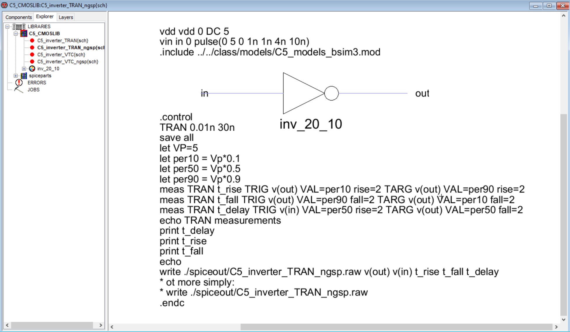 |
DRC the schematic (F5)
run the simulation (Shift S)
plot the simulation output (Alt S)
NOTE: if a spice input file contains a control section (.control … .endc), when running ngspice in batch mode (-b command line option) the -r rawfile command line option is ignored.
the raw file must be written from within the control section (./spiceout/C5_inverter_TRAN_ngsp.raw)
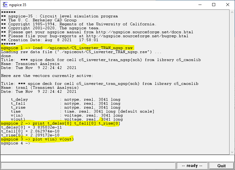
to see the inverter's dynamic parameters (t_rise, t_fall, t_delay) the fastest way is to browse the simulation log file or run ngspice from the CLI.
       ...
TRAN measurements
t_delay = 3.835032e-11
t_rise = 2.209172e-10
t_fall = 2.062974e-10
       ...
 |
 |