ring oscillator design, layout and simulation
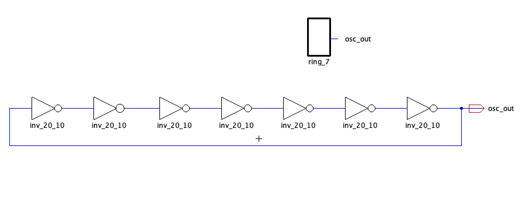
ring oscillator (7-stage) schematic
1. start electric
2. open the library C5_CMOSLIB
3. create the schematic view
Cell > New Cell
Name: ring_7
View: schematic
Technology: mocmos
4. drag (or copy ^C and paste ^V) the icon inv_20_10{ic} in the schematics
5. generate seven instances of the inv_20_10
Edit > Array | F6
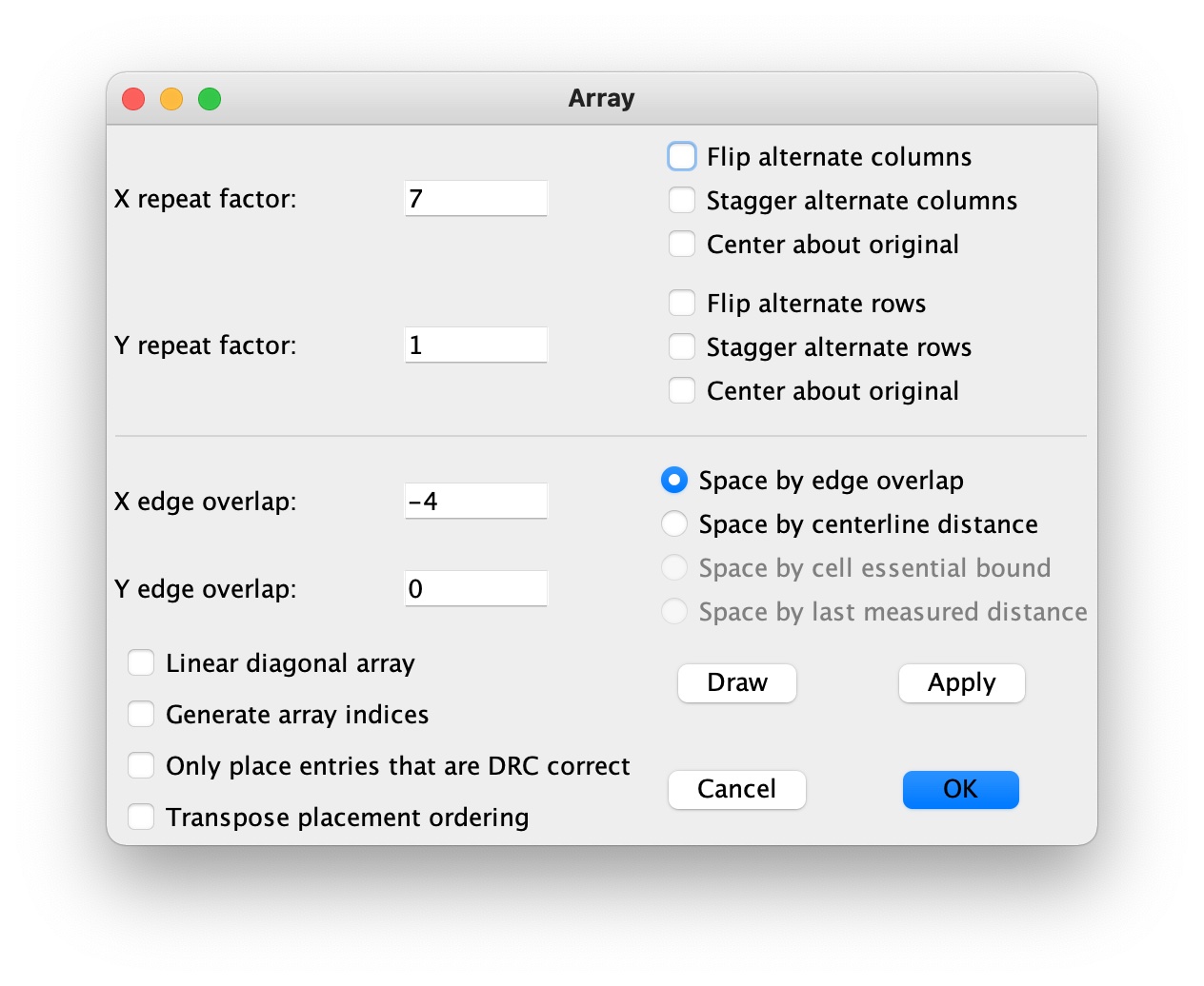 |
6. connect the inverters in a ring
7. add an off page connector to the output and export the output with the name osc_out
8. run DRC (F5)
9. make an icon view for ring_7
View > Make Icon View
 |
10. an alternative (faster) way to draw the schematic is to instatiate the inverter as a vector and then use bus wiring
Example: design and simulation of a 15-stage ring oscillator
instantiate the inverter icon as usual then change its name to be a vector (inverter[0:14])
connect the input and output ports using a bus
name the input bus osc_out,out[0:13]
name the output bus out[0,13],osc_out
run the simulation as usual
 |
 |
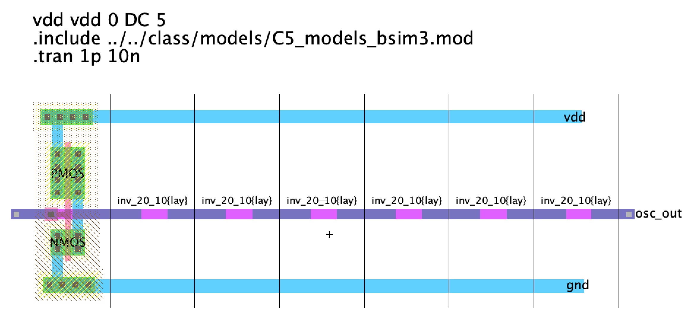
ring oscillator (7-stage) layout
1. create the Layout view
Cell > New Cell
Name: ring_7
View: layout
Technology: mocmos
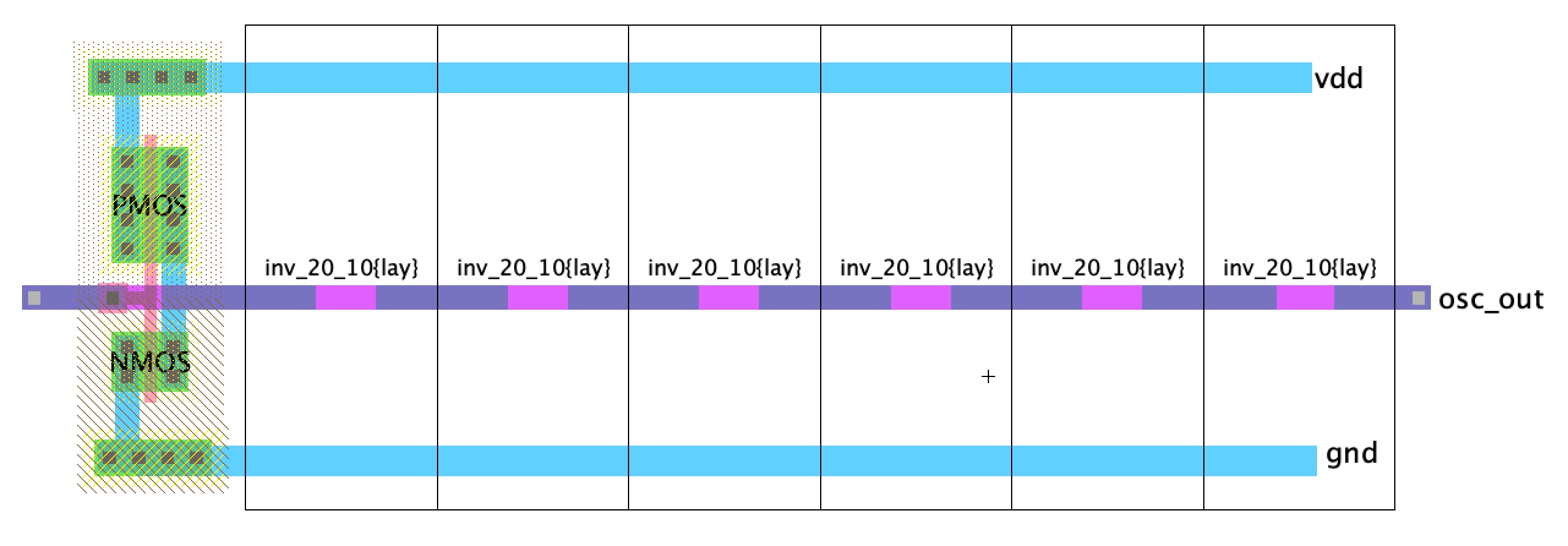
2. drag the layout inv_20_10{lay}
3. generate 7 instances of it
 |
 |
4. connect the inverters in a ring
add a Metal-1-Metal-2-Con close to the input of the first inverter and one close to the output of the last inverter
use Metal-1 to connect all vdd, all gnd, and all internal in and out ports of the inverters
use Metal-1 to connect the Metal-1-Metal-2-Con at the input of the first inverter to the first inverter's input
use Metal-1 to connect the Metal-1-Metal-2-Con at the output of the last inverter to last inverter;s output
use Metal-2 to connect the Metal-1-Metal-2-Con at the input of the first inverter with the Metal-1-Metal-2-Con at the output of the last inverter
export vdd, gnd, and osc_out
to check the exports use Export > List Exports or Export > Show Exports
 |
5. make sure the layout passes all checks, that is DRC, ERC, and NCC (a.k.a. LVS)
6. to change the level of details of the layout use
Cell > Expand Cell Instances or Cell > UnExpand Cell Instances or their equivalent shortcut icons
 |
 |
ring oscillator (7-stage) simulation
1. create a new cell to simulate the ring_7 oscillator schematic - ring_7_sim{sch}
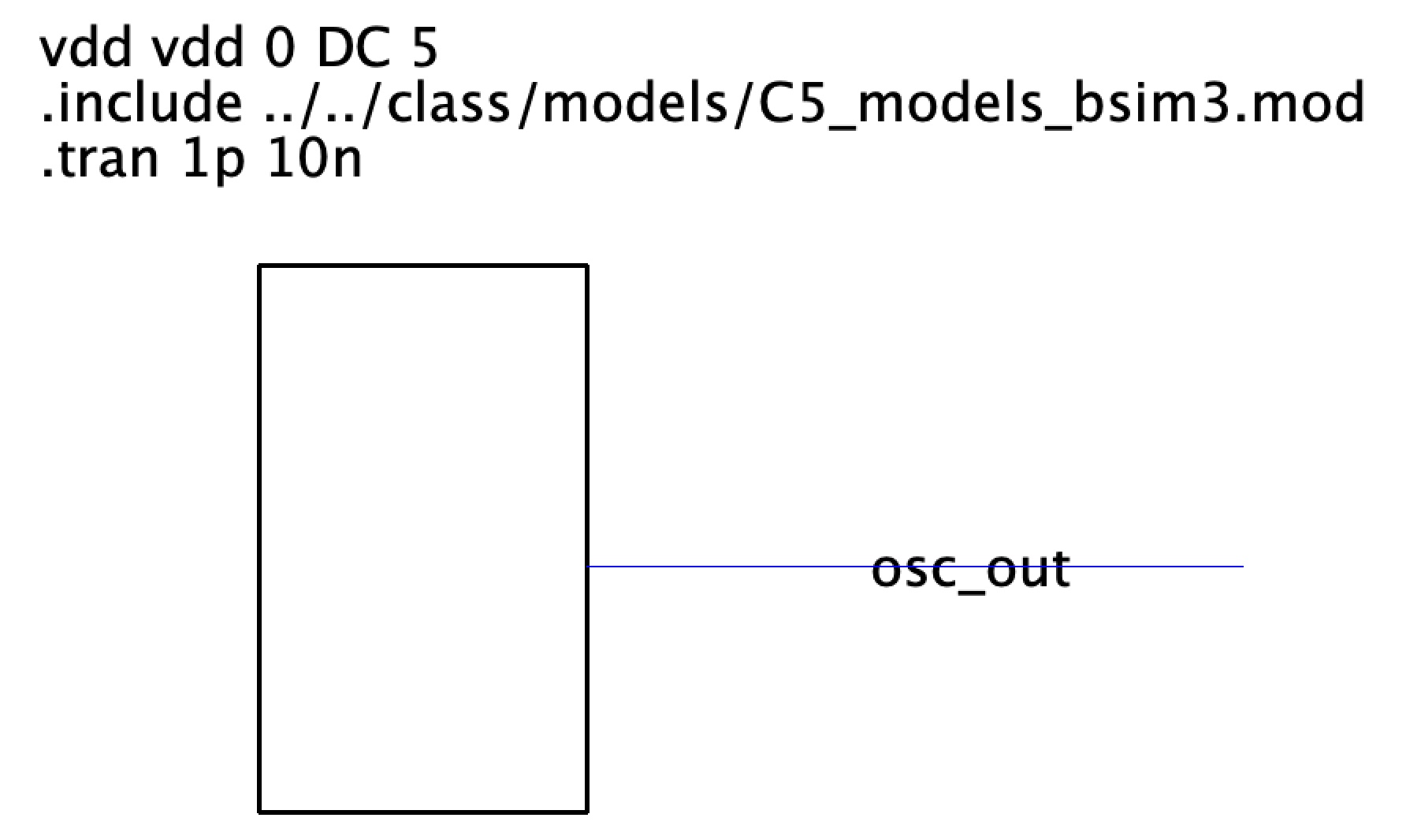 |
NOTE: osc_out is a wire's label
The netlist corresponding to the schematic is:
*** SPICE deck for cell ring_7_sim{sch} from library C5_CMOSLIB
*** Created on Fri Nov 26, 2021 12:53:38
*** Last revised on Fri Nov 26, 2021 21:22:37
*** Written on Fri Nov 26, 2021 21:23:04 by Electric VLSI Design System, version 9.07
*** Layout tech: mocmos, foundry MOSIS
*** UC SPICE *** , MIN_RESIST 4.0, MIN_CAPAC 0.1FF

*** SUBCIRCUIT C5_CMOSLIB__inv_20_10 FROM CELL inv_20_10{sch}
.SUBCKT C5_CMOSLIB__inv_20_10 in out
** GLOBAL gnd
** GLOBAL vdd
Mnmos@2 out in gnd gnd NMOS L=0.6U W=3U
Mpmos@0 vdd in out vdd PMOS L=0.6U W=6U
.ENDS C5_CMOSLIB__inv_20_10

*** SUBCIRCUIT C5_CMOSLIB__ring_7 FROM CELL ring_7{sch}
.SUBCKT C5_CMOSLIB__ring_7 osc_out
** GLOBAL gnd
** GLOBAL vdd
Xinv_20_1@1 osc_out net@13 C5_CMOSLIB__inv_20_10
Xinv_20_1@2 net@13 net@21 C5_CMOSLIB__inv_20_10
Xinv_20_1@3 net@21 net@0 C5_CMOSLIB__inv_20_10
Xinv_20_1@4 net@0 net@1 C5_CMOSLIB__inv_20_10
Xinv_20_1@5 net@1 net@2 C5_CMOSLIB__inv_20_10
Xinv_20_1@6 net@2 net@3 C5_CMOSLIB__inv_20_10
Xinv_20_1@7 net@3 osc_out C5_CMOSLIB__inv_20_10
.ENDS C5_CMOSLIB__ring_7

.global gnd vdd

*** TOP LEVEL CELL: ring_7_sim{sch}
Xring_7@1 osc_out C5_CMOSLIB__ring_7

* Spice Code nodes in cell cell 'ring_7_sim{sch}'
vdd vdd 0 DC 5
.include ../../class/models/C5_models_bsim3.mod
.tran 1p 10n
.END
NOTE: the schematic netlist does not include the transistors’ AD, AS, PD, and PS
2. create a new cell to simulate the inverter layout - inverter_sim{lay}
 |
make sure to export vdd, gnd, and osc_out
make sure to pass DRC, ERC, and NCC (a.k.a. LVS)
export all parasitics
Preferences > Tools > Spice/CDL
 |
The netlist corresponding to the layout is:
*** SPICE deck for cell ring_7_sim{lay} from library C5_CMOSLIB
*** Created on Fri Nov 26, 2021 21:02:08
*** Last revised on Fri Nov 26, 2021 21:29:38
*** Written on Fri Nov 26, 2021 21:31:19 by Electric VLSI Design System, version 9.07
*** Layout tech: mocmos, foundry MOSIS
*** UC SPICE *** , MIN_RESIST 4.0, MIN_CAPAC 0.1FF
***    P-Active:	areacap=0.9FF/um^2,	edgecap=0.0FF/um,	res=2.5ohms/sq
***    N-Active:	areacap=0.9FF/um^2,	edgecap=0.0FF/um,	res=3.0ohms/sq
***    Polysilicon-1:	areacap=0.1467FF/um^2,	edgecap=0.0608FF/um,	res=6.2ohms/sq
***    Polysilicon-2:	areacap=1.0FF/um^2,	edgecap=0.0FF/um,	res=50.0ohms/sq
***    Transistor-Poly:	areacap=0.09FF/um^2,	edgecap=0.0FF/um,	res=2.5ohms/sq
***    Poly-Cut:	areacap=0.0FF/um^2,	edgecap=0.0FF/um,	res=2.2ohms/sq
***    Active-Cut:	areacap=0.0FF/um^2,	edgecap=0.0FF/um,	res=2.5ohms/sq
***    Metal-1:	areacap=0.1209FF/um^2,	edgecap=0.1104FF/um,	res=0.078ohms/sq
***    Via1:	areacap=0.0FF/um^2,	edgecap=0.0FF/um,	res=1.0ohms/sq
***    Metal-2:	areacap=0.0843FF/um^2,	edgecap=0.0974FF/um,	res=0.078ohms/sq
***    Via2:	areacap=0.0FF/um^2,	edgecap=0.0FF/um,	res=0.9ohms/sq
***    Metal-3:	areacap=0.0843FF/um^2,	edgecap=0.0974FF/um,	res=0.078ohms/sq
***    Via3:	areacap=0.0FF/um^2,	edgecap=0.0FF/um,	res=0.8ohms/sq
***    Metal-4:	areacap=0.0843FF/um^2,	edgecap=0.0974FF/um,	res=0.078ohms/sq
***    Via4:	areacap=0.0FF/um^2,	edgecap=0.0FF/um,	res=0.8ohms/sq
***    Metal-5:	areacap=0.0843FF/um^2,	edgecap=0.0974FF/um,	res=0.078ohms/sq
***    Via5:	areacap=0.0FF/um^2,	edgecap=0.0FF/um,	res=0.8ohms/sq
***    Metal-6:	areacap=0.0423FF/um^2,	edgecap=0.1273FF/um,	res=0.036ohms/sq
***    Hi-Res:	areacap=0.0FF/um^2,	edgecap=0.0FF/um,	res=1.0ohms/sq

*** SUBCIRCUIT C5_CMOSLIB__inv_20_10 FROM CELL inv_20_10{lay}
.SUBCKT C5_CMOSLIB__inv_20_10 gnd in out vdd
Mnmos@1 out in#2nmos@1_poly-right gnd gnd NMOS L=0.6U W=3U AS=15.75P AD=7.425P PS=24.9U PD=12.3U
Mpmos@1 out in#0pmos@1_poly-left vdd vdd PMOS L=0.6U W=6U AS=20.7P AD=7.425P PS=30.9U PD=12.3U
** Extracted Parasitic Capacitors ***
C0 in 0 0.102fF
C1 out 0 3.403fF
C2 in#1pin@6_polysilicon-1 0 0.27fF
** Extracted Parasitic Resistors ***
R0 in#0pmos@1_poly-left in#0pmos@1_poly-left##0 6.2
R1 in#0pmos@1_poly-left##0 in#1pin@6_polysilicon-1 6.2
R2 in#1pin@6_polysilicon-1 in#1pin@6_polysilicon-1##0 6.2
R3 in#1pin@6_polysilicon-1##0 in#2nmos@1_poly-right 6.2
R4 in#1pin@6_polysilicon-1 in#1pin@6_polysilicon-1##0 6.717
C3 in#1pin@6_polysilicon-1##0 0 0.102fF
R5 in#1pin@6_polysilicon-1##0 in#1pin@6_polysilicon-1##1 6.717
C4 in#1pin@6_polysilicon-1##1 0 0.102fF
R6 in#1pin@6_polysilicon-1##1 in 6.717
.ENDS C5_CMOSLIB__inv_20_10

*** SUBCIRCUIT C5_CMOSLIB__ring_7 FROM CELL ring_7{lay}
.SUBCKT C5_CMOSLIB__ring_7 gnd osc_out vdd
Xinv_20_1@0 gnd osc_out#1inv_20_1@0_in net@0 vdd C5_CMOSLIB__inv_20_10
Xinv_20_1@1 gnd net@0 net@1 vdd C5_CMOSLIB__inv_20_10
Xinv_20_1@2 gnd net@1 net@2 vdd C5_CMOSLIB__inv_20_10
Xinv_20_1@3 gnd net@2 net@3 vdd C5_CMOSLIB__inv_20_10
Xinv_20_1@4 gnd net@3 net@4 vdd C5_CMOSLIB__inv_20_10
Xinv_20_1@5 gnd net@4 net@5 vdd C5_CMOSLIB__inv_20_10
Xinv_20_1@6 gnd net@5 osc_out vdd C5_CMOSLIB__inv_20_10
** Extracted Parasitic Capacitors ***
C0 osc_out 0 11.96fF
C1 osc_out#1inv_20_1@0_in 0 12.07fF
C2 net@0 0 2.031fF
C3 net@1 0 2.031fF
C4 net@2 0 2.031fF
C5 net@3 0 2.031fF
C6 net@4 0 2.031fF
C7 net@5 0 2.086fF
** Extracted Parasitic Resistors ***
R0 osc_out#1inv_20_1@0_in osc_out 4.651
.ENDS C5_CMOSLIB__ring_7

*** TOP LEVEL CELL: ring_7_sim{lay}
Xosc_out gnd osc_out vdd C5_CMOSLIB__ring_7
** Extracted Parasitic Capacitors ***
** Extracted Parasitic Resistors ***

* Spice Code nodes in cell cell 'ring_7_sim{lay}'
vdd vdd 0 DC 5
.include ../../class/models/C5_models_bsim3.mod
.tran 1p 10n
.END
NOTE: the layout netlist include the transistors’ AD, AS, PD, and PS, and the parasitics associated to the layout interconnections
3. run ngspice on both netlists and write the results in ./spiceout/ring_7_sim_sch.raw and ./spiceout/ring_7_sim_lay.raw
# Pyring_7_sim.py

from PyLTSpice.LTSpice_RawRead import RawRead as RawRead
import matplotlib.pyplot as plt
import numpy as np

LTR = RawRead("./spiceout/ring_7_sim_sch.raw")

print(LTR.get_trace_names())
print("\n")
print(LTR.get_raw_property())
print("\n")
steps = LTR.get_steps()
num_steps = len(steps)
print('number of sweeps in the simulation (sch):', num_steps)

# objects containing the data
t = LTR.get_trace('time')
Vo = LTR.get_trace('v(osc_out)')

# extract the data from the objects
if num_steps == 1:
   time_sch = t.get_time_axis(0)
   Vout_sch = Vo.get_wave(0)

LTR = RawRead("./spiceout/ring_7_sim_lay.raw")

print(LTR.get_trace_names())
print("\n")
print(LTR.get_raw_property())
print("\n")
steps = LTR.get_steps()
num_steps = len(steps)
print('number of sweeps in the simulation (lay):', num_steps)

# objects containing the data
t = LTR.get_trace('time')
Vo = LTR.get_trace('v(osc_out)')

# extract the data from the objects
if num_steps == 1:
   time_lay = t.get_time_axis(0)
   Vout_lay = Vo.get_wave(0)

fig1 = plt.figure()
plt.subplot(211) # 2 plots - col. 1, row 1
plt.title("7-stage ring oscillator: transient simulation (schematic)" )
plt.ylabel("voltage (V)")
plt.xlabel("time (ns)")
plt.plot(time_sch*1e9,Vout_sch, color='royalblue',
        label="v$_{out}$(t) \n$\it{schematic}$")
plt.legend(loc="upper left",frameon=True,fontsize=9)
plt.yticks(np.arange(0,5.1, step=1))

plt.subplot(212) # 2 plots - col. 1, row 2
plt.title("7-stage ring oscillator: transient simulation (layout)" )
plt.ylabel("voltage (V)")
plt.xlabel("time (ns)")
plt.plot(time_lay*1e9,Vout_lay, color='lightseagreen' ,
        label="v$_{out}$(t) \n$\it{layout}$")
plt.legend(loc="upper left",frameon=True,fontsize=9)
plt.yticks(np.arange(0,5.1, step=1))

plt.tight_layout();

plt.show()
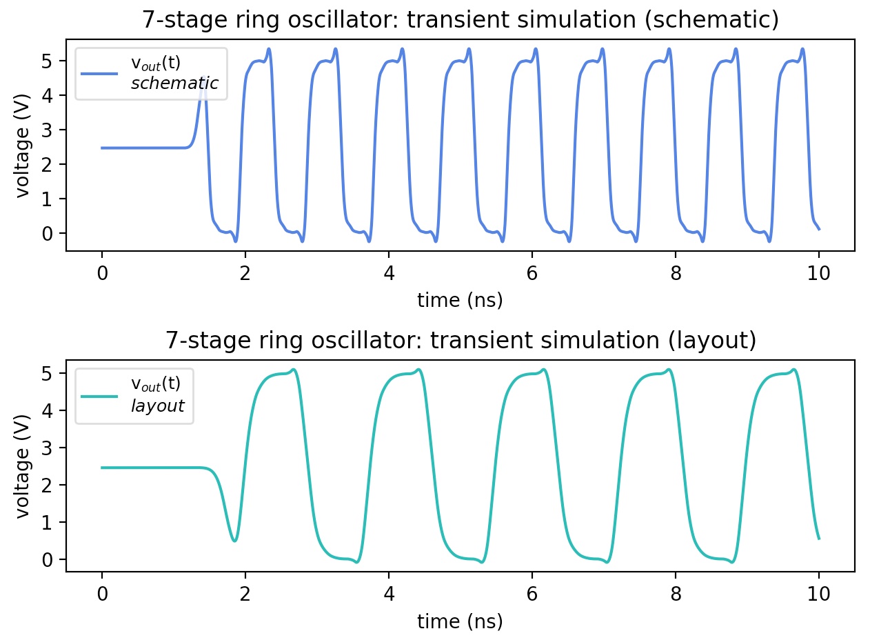 |
Note: due to the effect of the parasitics, the oscillation period is significantly slower than expected