inverter layout and post-layout simulation
creating the inverter layout
1. start electric
2. open the library C5_CMOSLIB
3. create the layout view to associate to the cell inv_20_10
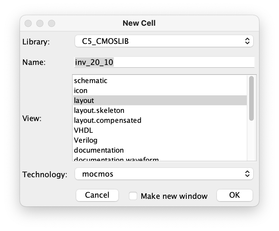
Cell > New Cell
Name: inv_20_10
View: Layout
Technology: mocmos
 |
 |
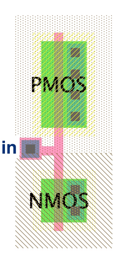
4. to layout the inverter we need the following components:
pMOS (P-Transistor)
nMOS (N-transistor)
Polysilicon-1
Metal-1-Polysilicon-1-Con
Metal-1
Metal-1-Pin
pAct (Metal-1-P-Active-Con)
nAct (Metal-1-N-Active-Con)
pWell (Metal-1-P-Well-Con)
nWell (Metal-1-N-Well-Con)
5. select the pMOS component
place the component
rotate the component by 90 degree
Edit > Rotate > 90 degrees Counterclockwisesize the component
Edit > Properties > Object Properties
width: 20
length: 2
set the spice model
Tools > Simulation (SPICE) > Set SPICE Model
select the name of the spice model and change it to PMOS
change the text size to 5
6. select the nMOS component
place the component
rotate the component by 90 degree
Edit > Rotate > 90 degrees Counterclockwisesize the component
Edit > Properties > Object Properties
width: 10
length: 2
set the spice model
Tools > Simulation (SPICE) > Set SPICE Model
select the name of the spice model and change it to NMOS
make the text size 5
 |
7. use polysilicon to connect the gates of the two transistors
8. add a Metal-1-Polysilicon-1-Con to create the input port of the inverter
select, place, and connect the Metal-1-Polysilicon-Con to the poly
export the connector:
Export > Create Export
Export name: In
select the name of the port, make the text size 4, and move the text
9. keep the layout as compact as possible
(move the components as close as possible w/o violating the design rules)
run DRC (Tools > DRC > Check hierarchically | F5)
 |
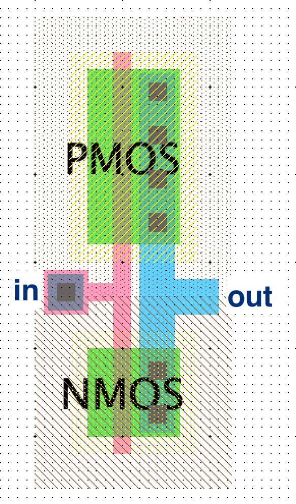
10. add a Metal-1-P-Active-Con (pAct) to the drain of the pMOS
select, place and connect the Metal-1-P-Active-Con to the drain
size the pAct component
Edit > Properties > Object Properties
Y size: 20
move the pAct as close as possible to the poly w/o violating DRC
11. add a Metal-1-N-Active-Con (nAct) to the drain of the nMOS
select, place, and connect the Metal-1-N-Active-Con to the drain
size the nAct component
Edit > Properties > Object Properties
Y size: 10
move the nAct as close as possible to the poly w/o violating DRC
 |
12. use metal to connect the drain of the pMOS and the drain of the nMOS
13. add a Metal-pin on the metal connection and create the output port of the inverter
select, place and connect the Metal-pin on the metal connection
export the metal pin:
Export > Create Export
Export name: Out
select the name of the port, make the text size 4, and move the text
 |
14. connect the p-well and the source of nMOS transistor to gnd
select, place, and size a Metal-1-N-Active-Con
connect the nAct to the source of the nMOS
select, and place a Metal-1-P-Well-Con (pWell component) in the well
use metal to connect the source of the nMOS transistor to the pWell component
export the pWell component Export > Create Export
Export name: gnd
make the text size 4
15. connect the n-well and the source of the pMOS transistor to vdd
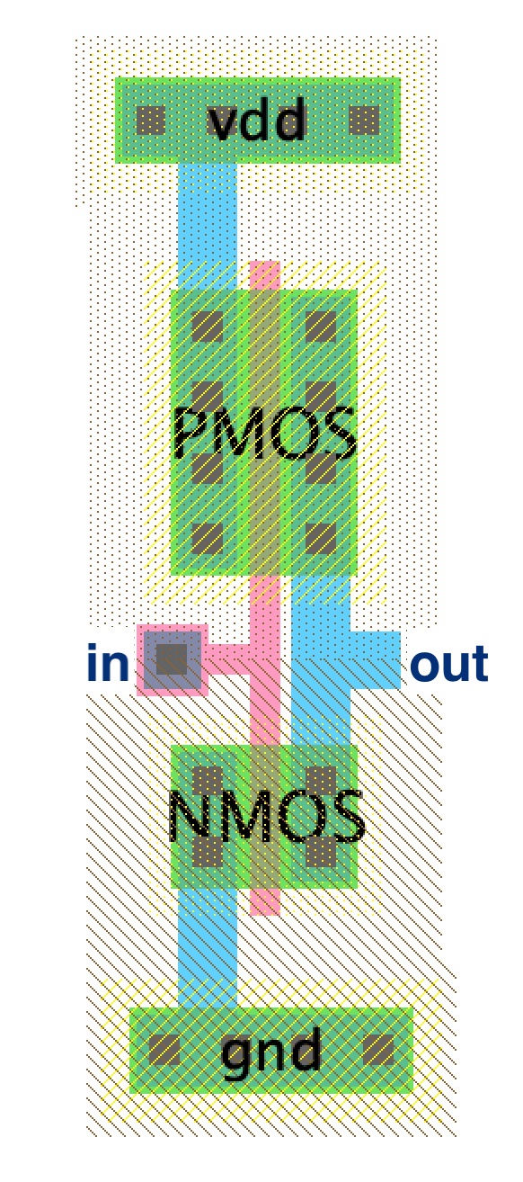 |
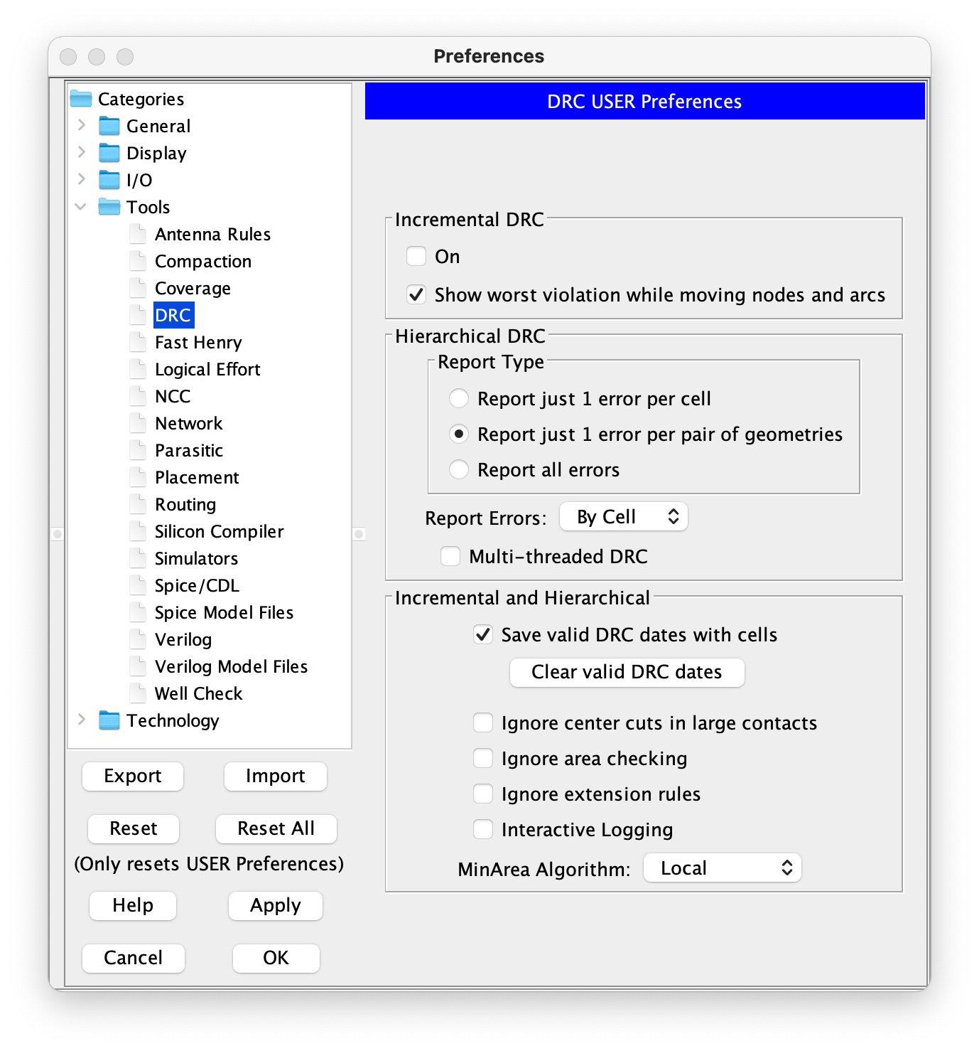
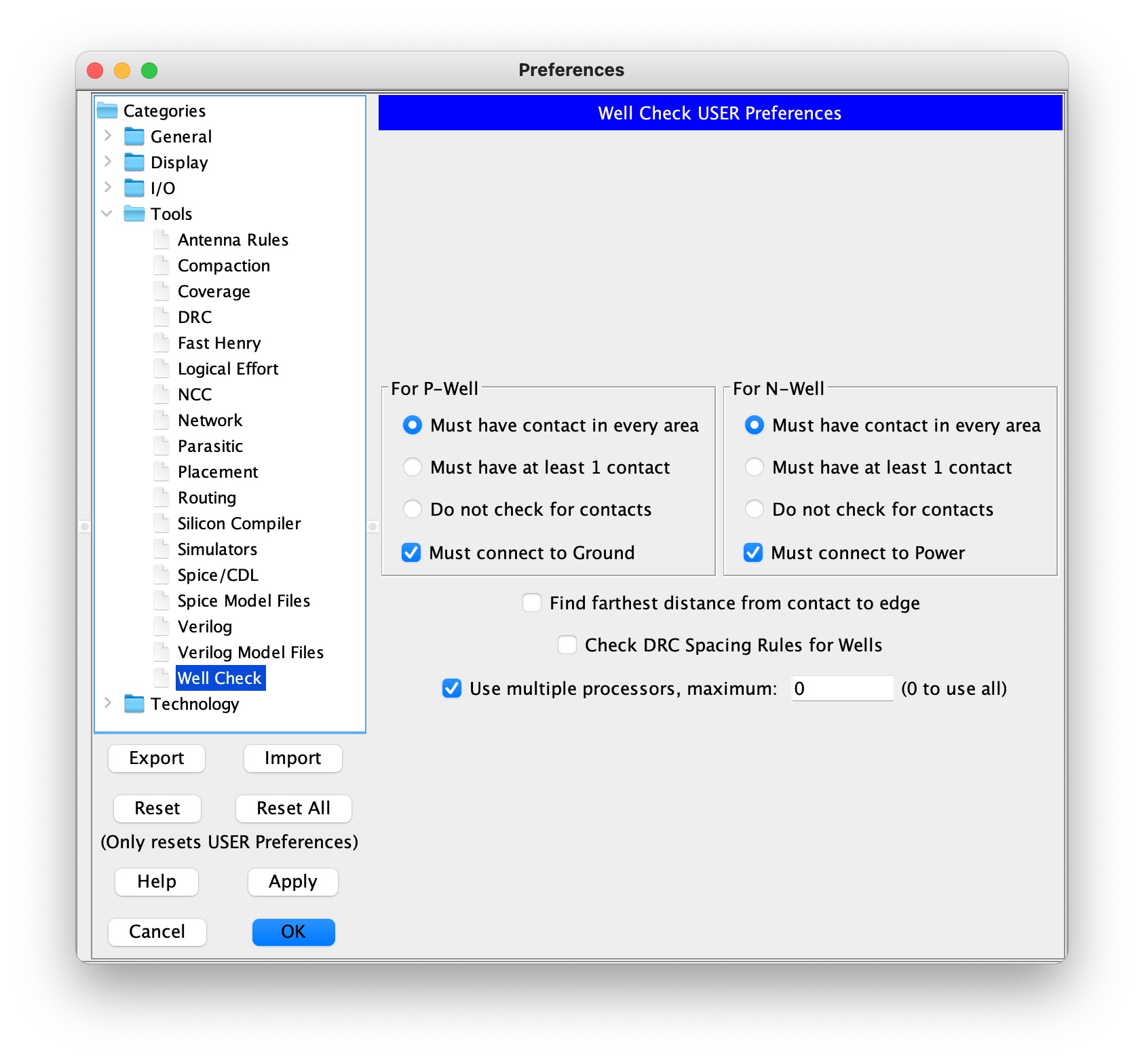
16. at this point the layout is complete
make sure the preferences required to check the layout are in compliance with all technology rules (design and electric rules)
and matches schematicFile > Preferences > Tools > DRC
 |
File > Preferences > Tools > Well Check
 |
File > Preferences > Tools > NCC
 |
run DRC (design rules check):
Tools > DRC > Check hierarchically | F5run ERC (electric rule check):
Tools > ERC > Check Wellsrun NNC (network compatibility check, also know as LVS = layout vs. schematic):
Tools > NCC > Schematic and Layout Views of Cell in Current Window
post-layout simulation
1. create a new cell to simulate the inverter schematic - inverter_sim{sch}
 |
The netlist corresponding to the schematic is:
*** SPICE deck for cell inverter_sim{sch} from library C5_CMOSLIB
*** Created on Fri Nov 19, 2021 00:37:00
*** Last revised on Wed Nov 24, 2021 15:20:24
*** Written on Wed Nov 24, 2021 15:56:38 by Electric VLSI Design System, version 9.07
*** Layout tech: mocmos, foundry MOSIS
*** UC SPICE *** , MIN_RESIST 4.0, MIN_CAPAC 0.1FF

*** SUBCIRCUIT C5_CMOSLIB__inv_20_10 FROM CELL inv_20_10{sch}
.SUBCKT C5_CMOSLIB__inv_20_10 in out
** GLOBAL gnd
** GLOBAL vdd
Mnmos@2 out in gnd gnd NMOS L=0.6U W=3U
Mpmos@0 vdd in out vdd PMOS L=0.6U W=6U
.ENDS C5_CMOSLIB__inv_20_10

.global gnd vdd

*** TOP LEVEL CELL: inverter_sim{sch}
Xinv_20_1@2 in out C5_CMOSLIB__inv_20_10

* Spice Code nodes in cell cell 'inverter_sim{sch}'
.include ../../class/models/C5_models_bsim3.mod
vdd vdd 0 dc 5
vin in 0 pulse (0 5 0 1n 1n 4n 10n)
.tran 100p 30n
.plot tran v(out) v(in)
.END
NOTE: the schematic netlist does not include the transistors’ AD, AS, PD, and PS
2. create a new cell to simulate the inverter layout - inverter_sim{lay}
 |
NOTE: since in the icon view of the inverter vdd and gnd are implied, in the layout view the metal connections to vdd and gnd must be exported, while the metal connections to the in and out ports are net labels
The netlist corresponding to the layout is:
*** SPICE deck for cell inverter_sim{lay} from library C5_CMOSLIB
*** Created on Fri Nov 19, 2021 01:03:23
*** Last revised on Wed Nov 24, 2021 15:54:32
*** Written on Wed Nov 24, 2021 15:56:12 by Electric VLSI Design System, version 9.07
*** Layout tech: mocmos, foundry MOSIS
*** UC SPICE *** , MIN_RESIST 4.0, MIN_CAPAC 0.1FF

*** SUBCIRCUIT C5_CMOSLIB__inv_20_10 FROM CELL inv_20_10{lay}
.SUBCKT C5_CMOSLIB__inv_20_10 gnd in out vdd
Mnmos@1 out in gnd gnd NMOS L=0.6U W=3U AS=15.75P AD=7.425P PS=24.9U PD=12.3U
Mpmos@1 out in vdd vdd PMOS L=0.6U W=6U AS=20.7P AD=7.425P PS=30.9U PD=12.3U
.ENDS C5_CMOSLIB__inv_20_10

*** TOP LEVEL CELL: inverter_sim{lay}
Xinv_20_1@4 gnd in out vdd C5_CMOSLIB__inv_20_10

* Spice Code nodes in cell cell 'inverter_sim{lay}'
.include ../../class/models/C5_models_bsim3.mod
vdd vdd 0 dc 5
vin in 0 pulse (0 5 0 1n 1n 4n 10n)
.tran 100p 30n
.plot tran v(out) v(in)
.END
NOTE: the layout netlist include the transistors’ AD, AS, PD, and PS
3. run ngspice on both netlists and write the results in ./spiceout/inverter_sim_sch.raw and ./spiceout/inverter_sim_lay.raw
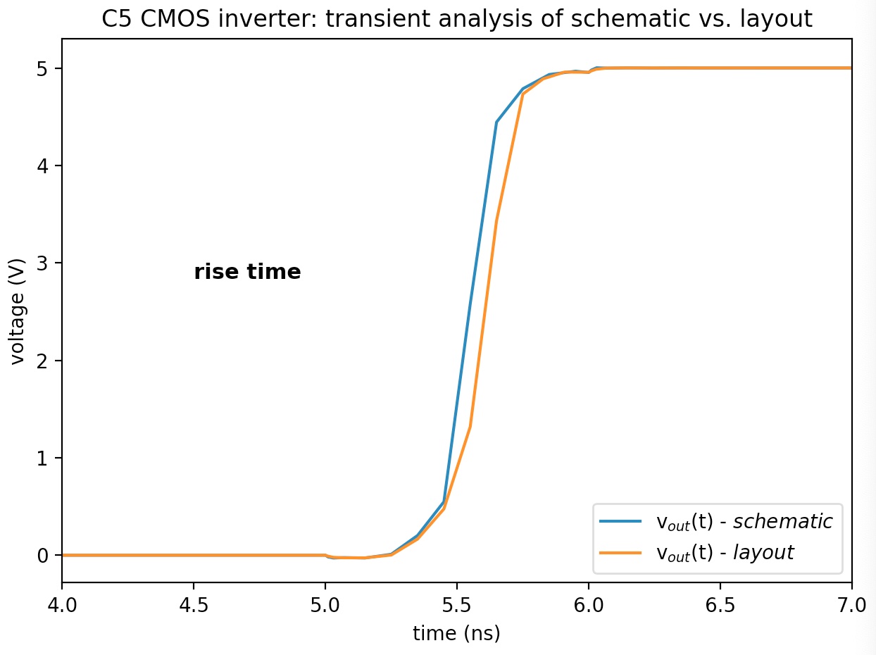
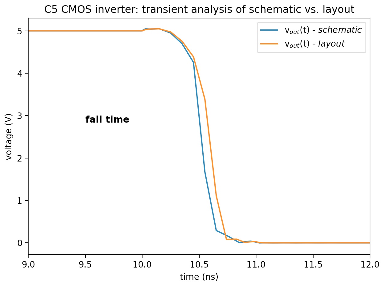
to better appreciate the effect AD, AS, PD and PS let's look at the simulation results
# Pyinverter_sim.py
from PyLTSpice.LTSpice_RawRead import RawRead as RawRead
import matplotlib.pyplot as plt
import numpy as np

LTR = RawRead("./spiceout/inverter_sim_sch.raw")

print(LTR.get_trace_names())
print("\n")
print(LTR.get_raw_property())
print("\n")
steps = LTR.get_steps()
num_steps = len(steps)
print('number of sweeps in the simulation (sch):', num_steps)

# objects containing the data
t = LTR.get_trace('time')
Vo = LTR.get_trace('v(out)')
Vi = LTR.get_trace('v(in)')

# extract the data from the objects
if num_steps == 1:
   time_sch = t.get_time_axis(0)
   Vout_sch = Vo.get_wave(0)
   Vin_sch = Vi.get_wave(0)

LTR = RawRead("./spiceout/inverter_sim_lay.raw")

print(LTR.get_trace_names())
print("\n")
print(LTR.get_raw_property())
print("\n")
steps = LTR.get_steps()
num_steps = len(steps)
print('number of sweeps in the simulation (lay):', num_steps)

# objects containing the data
t = LTR.get_trace('time')
Vo = LTR.get_trace('v(out)')
Vi = LTR.get_trace('v(in)')

# extract the data from the objects
if num_steps == 1:
   time_lay = t.get_time_axis(0)
   Vout_lay = Vo.get_wave(0)
   Vin_lay = Vi.get_wave(0)

fig1 = plt.figure()
plt.title("C5 CMOS inverter: transient analysis of schematic vs. layout" )
plt.ylabel("voltage (V)")
plt.xlabel("time (ns)")
plt.xlim([4,7])
str1 = "rise time"
plt.annotate(str1, xy=(4.5,3.0), ha='left', va='top', color='black',
        fontsize=11, weight='bold')
# plt.plot(time_sch*1e9,Vin_sch, label="v$_{in}$(t)")
plt.plot(time_sch*1e9,Vout_sch, label="v$_{out}$(t) - $\it{schematic}$")
plt.plot(time_lay*1e9,Vout_lay, label="v$_{out}$(t) - $\it{layout}$")
plt.legend(loc="lower right",frameon=True,fontsize=10)

plt.tight_layout();

fig2 = plt.figure()
plt.title("C5 CMOS inverter: transient analysis of schematic vs. layout" )
plt.ylabel("voltage (V)")
plt.xlabel("time (ns)")
plt.xlim([9,12])
str2 = "fall time"
plt.annotate(str2, xy=(9.5,3.0), ha='left', va='top', color='black',
        fontsize=11, weight='bold')
# plt.plot(time_sch*1e9,Vin_sch, label="v$_{in}$(t)")
plt.plot(time_sch*1e9,Vout_sch, label="v$_{out}$(t) - $\it{schematic}$")
plt.plot(time_lay*1e9,Vout_lay, label="v$_{out}$(t) - $\it{layout}$")
plt.legend(loc="upper right",frameon=True,fontsize=10)
plt.tight_layout();

plt.show()
 |
 |